



We are committed to protecting your personal data and providing you with access to your personal data in accordance with the personal data protection laws in force in the European Union.
By clicking "Accept All", you are allowing us to place cookies to enhance your experience on this website, to help us analyze site performance and usage, and to allow us to deliver relevant marketing content.
To learn more, please see our Privacy Policy
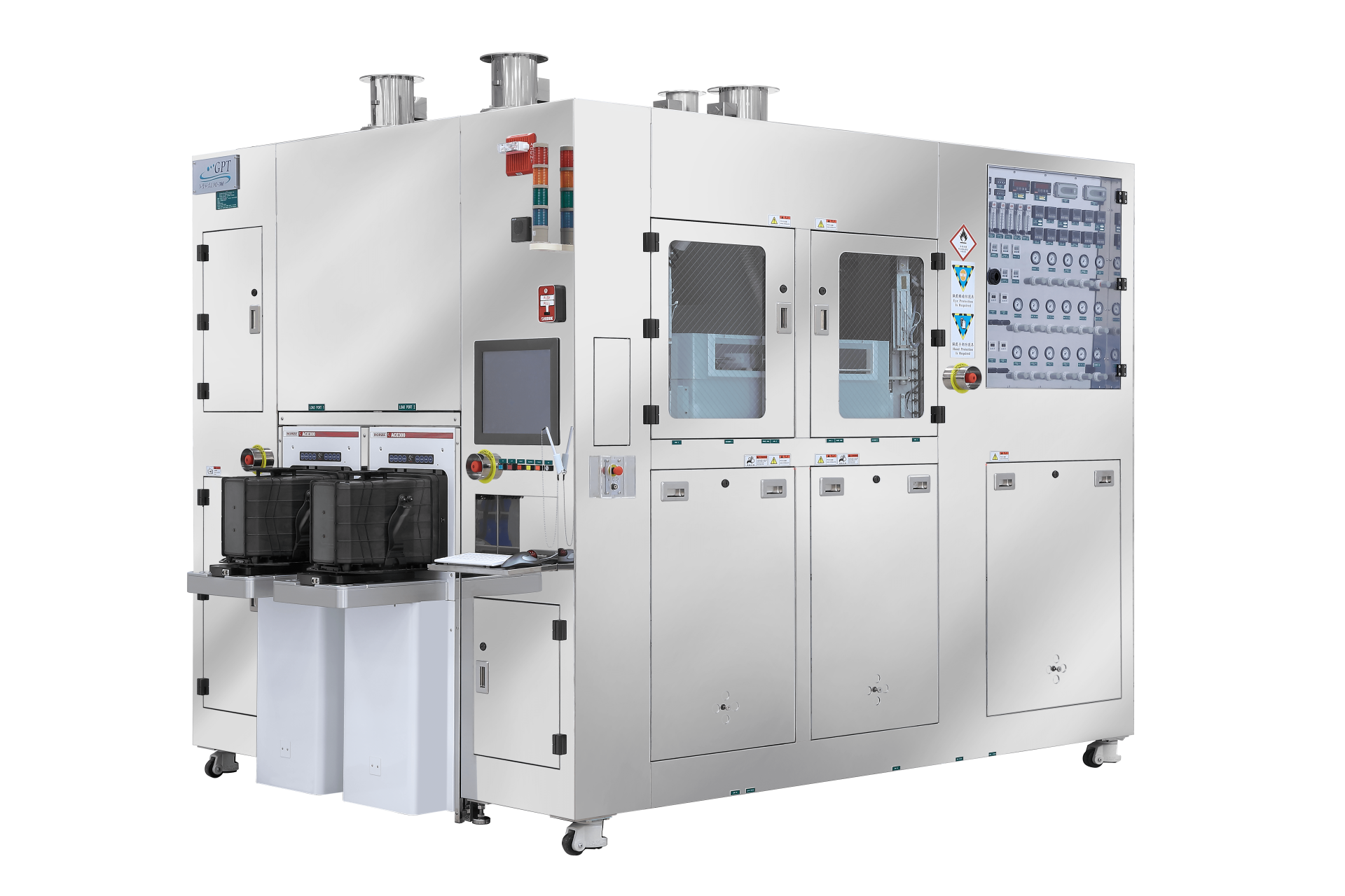
UFO-A Series
Process :
Etch, PR Strip, Wafer Cleaning
Solutions :
Advanced Semiconductor Packaging, 2.5D/3D IC Packaging, Compound Semiconductors, Silicon Wafer Manufacturing, SiC Wafer Manufacturing, MOSFET Backend Processes (BGBM)
Key Features:
- Integration of an etch endpoint detection system to enhance production efficiency and reduce manufacturing costs.
- Capability to incorporate a concentration monitoring system, ensuring process stability through precise chemical concentration control.
- Equipped with multi-layer chemical recycling rings and a chemical solution recovery mechanism, supporting continuous processing requirements while reducing chemical usage and lowering production costs.
- Static electricity protection mechanism to prevent process defects caused by electrostatic discharge.
- Specifically designed for handling highly warped wafers, effectively addressing wafer transport and clamping challenges.
- Customizable solutions for addressing process challenges related to chemical viscosity, foaming, residue, and other characteristics.
- Optimized process chamber flow field design, complemented by two-fluid soft spray cleaning, to enhance wafer cleanliness.
- Customizable options for acid mixing, preheating, and supply to accommodate diverse process needs.
- Integration of an etch endpoint detection system to enhance production efficiency and reduce manufacturing costs.
- Capability to incorporate a concentration monitoring system, ensuring process stability through precise chemical concentration control.
- Equipped with multi-layer chemical recycling rings and a chemical solution recovery mechanism, supporting continuous processing requirements while reducing chemical usage and lowering production costs.
- Static electricity protection mechanism to prevent process defects caused by electrostatic discharge.
- Specifically designed for handling highly warped wafers, effectively addressing wafer transport and clamping challenges.
- Customizable solutions for addressing process challenges related to chemical viscosity, foaming, residue, and other characteristics.
- Optimized process chamber flow field design, complemented by two-fluid soft spray cleaning, to enhance wafer cleanliness.
- Customizable options for acid mixing, preheating, and supply to accommodate diverse process needs.