












We are committed to protecting your personal data and providing you with access to your personal data in accordance with the personal data protection laws in force in the European Union.
By clicking "Accept All", you are allowing us to place cookies to enhance your experience on this website, to help us analyze site performance and usage, and to allow us to deliver relevant marketing content.
To learn more, please see our Privacy Policy
Advanced IC Packaging
Advanced IC Packaging
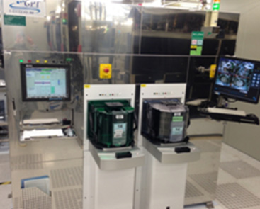
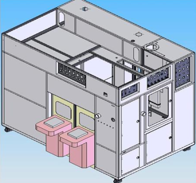
Wafer bumping is an essential process for flip chip packaging. GPTC has invested significantly in the research and development the equipment for wafer bumping.
UBM Etcher
Flip-chip Packaging Application Wafer bumping is an essential process for flip chip packaging.GPTC specializes in the research and development of high-performance wafer bumping equipment
PR Stripper
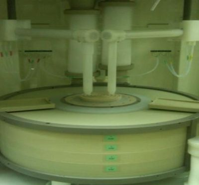
GPTC's PR stripper single-wafer equipment is designed for effective photoresist removal from 12-inch or 8-inch wafers during wet etching
Dry Film Stripping
Since the negative photoresist to produce cross-linking action (Cross-linking), difficult to remove photoresist comparison, conventional photoresist stripping agent (PR Stripper) of NMP (N-methyl-pyrrolidinone)
Flux Clean
Application of the packaging process in that the flux cleaning, provide bumps on Reflow process, a clean surface. Flux uses to promote the mobility of the tin-lead, usually in the flux will add some acids to increase their activity
Wafer Clean
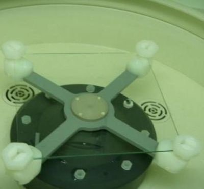
Scrubber(Wafer clean) water cleaning machine is wafer surface to remove dust particles from outside wafer surface (particle)
Laser de-bond cleaner
Debonding is the temporary bonding of wafers to a glass carrier to enable the next production sequence: back thinning
Mask Clean
GPTC provides quality, high-performance material handling solutions for photomask cleaning, prime wafer cleaning and stress release in front end process applications
IC Front End of Line, FEOL
GPTC provides material handling solutions for photomask cleaning, prime wafer cleaning and stress release in front end process.
EUV Mask Cleaner
Cleaned photomasks are essential for improved product yield. GPTC's expertise in cleaning and drying ensures professional photomasks cleanliness
Prime Wafer Cleaning Process
Cleaning wet chemical cleaning (Wet Cleaning) technology to remove particulate material Xipian surfaces, organic or inorganic and the like
Wafer Stress Release Etching Process
Silicon wafer back grinding defects arising generally include: grinding damage layer (damaged layer), crystal defects (Crystal Defect) and micro-cracks (Micro-crack), etc., through the silicon wet etc
Optoelectronics Applications
In photoelectric industry, GPTC provides the application for GeAs wet etching, PSS phosphoric acid etching, RCA cleaning and roughness process.
GaAs Etcher
Gallium arsenide is used in the manufacture of devices such as high frequency integrated circuits. GPTC provides single wafer equipment for GaAs wet etching process solution
PSS High-temperature Phosphoric Acid Etching Process
Using standard lithography and dry etching to etch part of the P-type GaN layer, to expose the N-type GaN layer, and thus define light emitting regions and the electrode
RCA Clean Manufacturing Process
Semiconductor wafer manufacturing process has five pollutants: particulate, metallic impurities, organic pollutants and naturally occurring oxide layer on the wafer surface micro-roughness
Micro-Roughness Surface Etching
The first step in the manufacture of solar cells is wafer cleaning (Wafer Cleaning). After cleaning the wafer, the surface to be roughened (Texture) process, since a flat silicon surface cause some re