



We are committed to protecting your personal data and providing you with access to your personal data in accordance with the personal data protection laws in force in the European Union.
By clicking "Accept All", you are allowing us to place cookies to enhance your experience on this website, to help us analyze site performance and usage, and to allow us to deliver relevant marketing content.
To learn more, please see our Privacy Policy
PSS High-temperature Phosphoric Acid Etching Process
In recent years, group III nitride (III-Nitride) high-brightness light-emitting diodes (HB-LED) have received growing attention. HB-LEDs are now widely used in traffic signals, LCD backlights, and various other lighting devices. The gallium nitride (GaN) LED is grown epitaxially on a sapphire substrate. The GaN epitaxial growth, the lattice constant of the sapphire substrate and the coefficient of thermo expansion (CTE) at the bottom are very different. This causes a high-density thread dislocation and limits the GaN LED’s luminous efficiency.
Wet chemical etching of patterned sapphire substrates (PSS) increases light extraction frequency. This is because substrate surface geometric pattern change can transform LED light diffusion mechanism. The change can also guide diffused light inside the LED and allow the light to exit through the escape angle.
Figure 1 is a diagram of the conventional LED and PPS LED current-light output power curve. When operating at a 20mA current, conventional LED and PPS LED outputs are 7.8 mW and 9 mW, respectively. The PPS LED output is 1.15 times higher than that of the conventional LED. In addition, when operating at a 20 mA current, the external quantum efficiency for conventional LEDs and PPS LEDs was 14.2% and 16.4%, respectively, and the PPS LED external quantum efficiency was also 1.15 times higher than that of conventional LEDs.
Wet chemical etching of patterned sapphire substrates (PSS) increases light extraction frequency. This is because substrate surface geometric pattern change can transform LED light diffusion mechanism. The change can also guide diffused light inside the LED and allow the light to exit through the escape angle.
Figure 1 is a diagram of the conventional LED and PPS LED current-light output power curve. When operating at a 20mA current, conventional LED and PPS LED outputs are 7.8 mW and 9 mW, respectively. The PPS LED output is 1.15 times higher than that of the conventional LED. In addition, when operating at a 20 mA current, the external quantum efficiency for conventional LEDs and PPS LEDs was 14.2% and 16.4%, respectively, and the PPS LED external quantum efficiency was also 1.15 times higher than that of conventional LEDs.

Figure 1、Diagram of current-light power output curves for conventional LEDs and PPS LEDs
The wet chemical etching process for patterned sapphire substrate (PSS) is as follows:
| item | PSS Process Flow |
|---|---|
| 1 | Desired pattern is produced on sapphire substrate using photolithography process |
| 2 | SiO2 is deposited on sapphire substrate using (PE-CVD). Patterns of arrays at 3μm apart are formed after photoresist removal |
| 3 | SiO2 is used as etching mask; the wet chemical etching of PPS is mixed with phosphoric acid and sulfuric acid at 280 °C. (Figure 5 is a cross-section view of a PSS after wet chemical etching. Fig. 6 is an optical microscope photograph) |
| 4 | Using MO-CVD to deposit GaN-LED on sapphire (001) plane, which is patterned by wet chemical etching. From the substrate, the GaN-LED structure consists of: GaN nucleation layer, undoped GaN layer, N-type GaN layer, luminescent layer (MQW), and P-type GaN layer |
| 5 | Part of P-type GaN layer is etched with standard lithography and dry etching. This will expose N-type GaN layer, and thus define light emitting regions and electrode. After patterned sapphire substrate undergoes wet etching, the epitaxy layer is deposited on patterned sapphire substrate. After PPS, epitaxial layer of GaN LED structure is deposited as shown in Figure 4 |
-
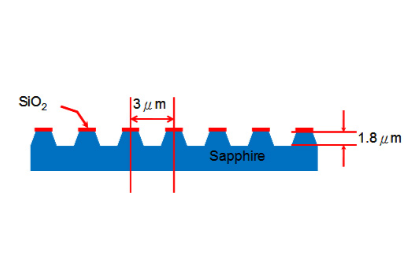 Figure 2、PSS after wet chemical etching cross-sectional view (Source: GPTC)
 -
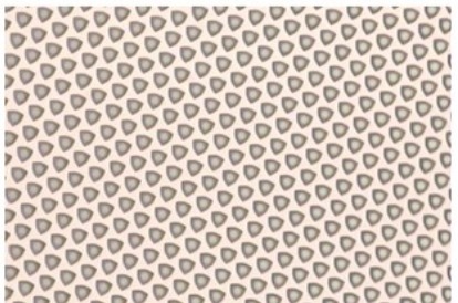 Figure 3、Optical microscope (OM) photo of PSS, after wet chemical etching (Source: GPTC WBD)
 -
 Figure 4、After PPS, the epitaxy layer of the GaN LED structure is grown
GPTC makes fully automated wet high-temperature phosphoric acid etching equipment (Fig. 5). It operates at a high temperature of 280–300 °C. The process has seven key designs:
| item | Design Highlights |
|---|---|
| 1.Safety design | Meet SEMI S2-200 certification standards. Personnel and product loading and off-loading areas are separated. This can ensure personnel safety. Exhaust gas would goes through ventilation to ensure air cleanliness |
| 2.High capacity design | Can load up to 200 wafers at once. That’s 2.75 times more than the equipment by other manufacturers |
| 3. Multi-tank design | The equipment has many sets of phosphoric acid tanks. When you use one group of tanks for etching, you can replace and heat the acid in another group of tanks. This feature saves time and money |
| 4.Heating and temperature control | The outside of the quartz tank has a thin heater layer, so heat is distributed uniformly through the tank. This can prevent temperature gradient and variations in etching rate so there will not be local thermal stresses on the wafer. If sapphire substrate is treated by high-temperature phosphoric acid wet chemical etching, the thickness can be precisely controlled at 1.9 ± 0.1μm, and the etching rate at 27.5 sec ± 0.5 angstroms |
| 5.Temperature elevation speed control | Pre-heating before wafer etching and cooling down after etching can prevent wafer breakage because of thermal variation |
| 6.Chemical supply system | Measure the volume of supplementary chemical solution with higher accuracy |
| 7. Automatic wafer transfer | We guarantee wafer transportation is continuous and smooth. Manufacturing yields are good |
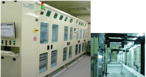
Figure 5、Automated high-temperature phosphoric acid wet etching equipment designed and manufactured by GPTC (Source: GPTC WBD)