



We are committed to protecting your personal data and providing you with access to your personal data in accordance with the personal data protection laws in force in the European Union.
By clicking "Accept All", you are allowing us to place cookies to enhance your experience on this website, to help us analyze site performance and usage, and to allow us to deliver relevant marketing content.
To learn more, please see our Privacy Policy
Laser de-bond cleaner
Wafer bonding (Wafer Bonding) is one of the most crucial steps in 3D IC integration; wafers are aligned and bonded during this step to ensure a successful layer-to-layer interconnections. Many wafer bonding processes came from MEMS (Micro Electro Mechanical Systems). Nevertheless, the precision level of 3D IC wafer bonding technologies are five to ten times more advanced than MEMS. Bond alignment accuracy of extremely advanced 3D IC products can reach micron - even sub-micron level. Here are the steps in wafer bonding: surface patterning and cleaning, alignment, bonding, post-bond metrology.
Wafer-bonding consists of the following:
Wafer-bonding consists of the following:
- silicon-direct or fusion bonding.
- metal-metal bonding.
- polymer adhesive bonding.
To promote 3D IC manufacturing capabilities, GPTC designed the single wafer processor for backend packaging applications.
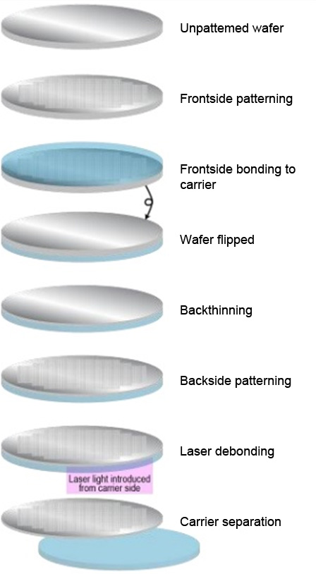
Figure 1、A schematic of the key process steps for thin wafer processing
GPTC has integrated several critical clean applications to remove residual adhesive after wafer debonding. To overcome issues with high warpage, and frontside/backside cleaning, GPTC developed a wafer flipping module and wafer bonder to ensure thorough cleaning. Further, GTPC has also designed an innovative Chuck system (wafer holder) to address uneven surfaces on wafer's frontside and backside.
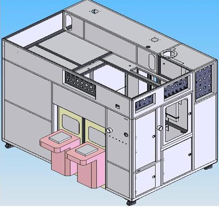
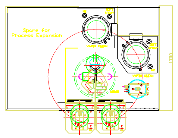
圖2、A schematic of GPTC's laser debond cleaner