



We are committed to protecting your personal data and providing you with access to your personal data in accordance with the personal data protection laws in force in the European Union.
By clicking "Accept All", you are allowing us to place cookies to enhance your experience on this website, to help us analyze site performance and usage, and to allow us to deliver relevant marketing content.
To learn more, please see our Privacy Policy
UBM Etcher
 Figure 1、Flow chart of tin-lead bumps deposition in flip chip technology
Figure 1 shows a flowchart of tin-lead bumps deposition in flip chip technology: photoresist removal and UBM etch are administered after tin-lead bumps are plated. In UBM etching, bumps or photoresist serve as an etching mask. The uncovered metal layer of the UBM is removed through the etching process to isolate individual bumps.
This is a critical process in flip chip technology, because incomplete UBM etch would cause electrical short circuit. On the other hand, excessive UBM etching would result in undercuts; worse, it could even etch into the bump, and damage the reliability of electronic components.
This is a critical process in flip chip technology, because incomplete UBM etch would cause electrical short circuit. On the other hand, excessive UBM etching would result in undercuts; worse, it could even etch into the bump, and damage the reliability of electronic components.
 Figure 2、GPTC's single-wafer spin etcher (UFO-300 series)
In general, a single-wafer spin etcher is used in the UBM etching process, as shown in Figure 2.Figure 2 shows GPTC's UFO-300 series
Different etching approaches should be applied during UBM etching, depending on the type and thickness of UBM metal layers, the chemical properties of the etching solutions, and patterns of the bump, to achieve the best etch uniformity.
Different etching approaches should be applied during UBM etching, depending on the type and thickness of UBM metal layers, the chemical properties of the etching solutions, and patterns of the bump, to achieve the best etch uniformity.
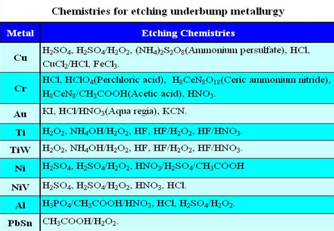
Table 1、Information on chemicals commonly used in UBM etching
The development of UBM etch chemical solutions is met with many challenges, due to the fact that the UBM layer has to be selectively etched, and that bumps (Bump) have to stay intact. Why is it that the UBM etch bump not be damaged? The reasons are as follows:
(2) to prevent the active phase of tin-lead bumps from premature dissolution, resulting in undesirable changes in bump's chemical composition.
(3) to prevent the surface of the tin-lead bumps from roughening, thus hindering the electrical test and probe sorting.
The selecting of the metal layer in UBM has grown more uniform over progressive evolution: Cu is applied to the wetting layer, and Ti or TiW for the barrier layer.
(1) to prevent volume loss of tin-lead bumps.
(2) to prevent the active phase of tin-lead bumps from premature dissolution, resulting in undesirable changes in bump's chemical composition.
(3) to prevent the surface of the tin-lead bumps from roughening, thus hindering the electrical test and probe sorting.
The selecting of the metal layer in UBM has grown more uniform over progressive evolution: Cu is applied to the wetting layer, and Ti or TiW for the barrier layer.
Copper (Cu) metal etching
Copper chloride is the most common copper etching solution in PCB industrial applications. Etching solution regeneration and an automatic supplement feature are required to ensure etching rate consistency. Unfortunately, tin-lead alloy can be easily etched by copper chloride etching; even if the etching solution contains a thin trace of chlorine ions, the ions would easily penetrate grain boundaries, or surface defects (such as pinholes), causing stress-type corrosion. In thermal cycling, performance efficiency of the components would suffer, shortening their lifetime Etching solutions must be chlorine-free to prevent the corrosion of the tin-lead bumps.
Copper(II) chloride is not applicable in microelectronics; Ammonium persulfate is the most common alternative, even though it damages tin-lead bump, it does not persistently corrode, nor does it affect etching rate. This is why Ammonium persulfate is the most common etching solution. Phosphoric acid solutions are used in some cases, but these solutions affect etching rate, and are not widely acceptable.
We use HF-based etching solution because HF is less likely to attack Cu or Pb than HCI-based solution.
Copper(II) chloride is not applicable in microelectronics; Ammonium persulfate is the most common alternative, even though it damages tin-lead bump, it does not persistently corrode, nor does it affect etching rate. This is why Ammonium persulfate is the most common etching solution. Phosphoric acid solutions are used in some cases, but these solutions affect etching rate, and are not widely acceptable.
We use HF-based etching solution because HF is less likely to attack Cu or Pb than HCI-based solution.
Titanium (Ti) and titanium tungsten (TiW) UBM etch
UMB (Ti or TiW) has two functions, one of which is adhesion, and the other serves as the barrier layer. High etching rate on UBM is necessary. Meanwhile, the UBM etching won't damage the final metal layer and passivation layer. We choose HF-based etching solution because HF is less likely to attack Cu or Pb than HCl-based solution. Titanium etching solution commonly used in microelectronics is predominantly a hydrofluoric acid-based solution. Such etchants would not attack copper (Cu) and aluminum (Pb). It has been widely applied in high-lead and high-tin bump materials following composition modification.
HF-based etching solution will cause significant undercut, and damage Al pad as well. Some people abandon HF-based solution and switch to H2O2-based solution. Unfortunately, H₂O₂ is unstable in high-pH environment.
High pH is alkaline in nature, making it a challenge for unstable environments. For example, in the delivery path, H₂O₂ would naturally produce bubbles, which interferes with the flow rate detection, even causing undesirable dripping on the nozzle. H₂O₂ causes bubbling and rising temperature, and it affects the etching rate. This is why pre-mix solutions are not acceptable. The solutions have to be mixed onsite during etching.
Hydrogen peroxide is principally used as solution for etching the TiW layer. Detta et al developed a chemical etching process that used hydrogen peroxide as main component. TiW is etched in the presence of PbSn, CrCu, Cu, and Al. 50 ℃is the operating temperature of such solutions, which contain the following ingredients: (1) hydrogen peroxide as etchant; (2) to potassium sulfate as a passivating agent to protect PbSn; (3) potassium - EDTA serves as the stabilizer for hydrogen peroxide, and doubles as the buffering agent and complex chemical compound for etched residues.
The nature of UMB layer, the structure and the thickness of the metal, the chemical properties of the etching solution and the distribution of the bump patterns must be taken into consideration for various etching methods when the manufacturer evaluates his priorities in UBM etching technologies to ensure optimum uniformity and minimize undercuts: the rotation speed of the wafer, the way the spray acid is processed, the selection of tubing material, and etchant flow control. As equipment manufacturers, we must stay ahead of the trend in packaging, and constantly reinvent our products to ensure our competitive edge, while keeping taps on our competitors to successfully meet the needs of wafer-level packaging market.
HF-based etching solution will cause significant undercut, and damage Al pad as well. Some people abandon HF-based solution and switch to H2O2-based solution. Unfortunately, H₂O₂ is unstable in high-pH environment.
High pH is alkaline in nature, making it a challenge for unstable environments. For example, in the delivery path, H₂O₂ would naturally produce bubbles, which interferes with the flow rate detection, even causing undesirable dripping on the nozzle. H₂O₂ causes bubbling and rising temperature, and it affects the etching rate. This is why pre-mix solutions are not acceptable. The solutions have to be mixed onsite during etching.
Hydrogen peroxide is principally used as solution for etching the TiW layer. Detta et al developed a chemical etching process that used hydrogen peroxide as main component. TiW is etched in the presence of PbSn, CrCu, Cu, and Al. 50 ℃is the operating temperature of such solutions, which contain the following ingredients: (1) hydrogen peroxide as etchant; (2) to potassium sulfate as a passivating agent to protect PbSn; (3) potassium - EDTA serves as the stabilizer for hydrogen peroxide, and doubles as the buffering agent and complex chemical compound for etched residues.
The nature of UMB layer, the structure and the thickness of the metal, the chemical properties of the etching solution and the distribution of the bump patterns must be taken into consideration for various etching methods when the manufacturer evaluates his priorities in UBM etching technologies to ensure optimum uniformity and minimize undercuts: the rotation speed of the wafer, the way the spray acid is processed, the selection of tubing material, and etchant flow control. As equipment manufacturers, we must stay ahead of the trend in packaging, and constantly reinvent our products to ensure our competitive edge, while keeping taps on our competitors to successfully meet the needs of wafer-level packaging market.